November 2, 2026Journal entry
We designed an 8-layer Rockchip board in Fusion 360
Why I build boards in Fusion 360, what that cost us on an 8-layer design with DDR and a BGA, and the scripts we wrote to make it work.
By Andrew Douglass · Founder

Disclosure: Our articles contain affiliate links, including Amazon. If you buy through one, we may earn a commission at no extra cost to you, and as an Amazon Associate we earn from qualifying purchases. It never affects our testing, measurements, or verdicts. Full disclosure.
Our RK3566 board is 8 layers, a fine-pitch BGA processor, DDR3L and a lot of controlled-impedance routing, and we designed all of it in Fusion 360. Not KiCad, not Altium. This entry is about why, what that cost us, and whether I would do it again.
The short answer: Fusion was the right tool for me to start in, because the board and the enclosure live in the same model. It was the wrong tool for impedance work, and we built our way around most of its gaps. I would not tell a new team to start there.
How I ended up in Fusion
I started using Fusion 360 in college, right when it came out, for a very practical reason: Autodesk was offering $250 gift cards to people who used it to model complex assemblies from provided drawings, and I needed the money. I had been using Creo before that, and Fusion was free for hobbyists, so I kept using it through college.
When Autodesk folded EAGLE into Fusion, I was working at SpaceX and itching to learn something new and design my own products, so I taught myself PCB design in it. It was a natural fit. I could sketch a board outline from the mechanical assembly, lay out the PCB, pull 3D models into the parts library, and drop the finished board back into the assembly to check fit. That loop is the whole reason I am still here.
It also surprises people. When I posted this board on r/embedded, a few of the replies were about the tool, not the board. One read: "The fact you did this in Fusion 360 just gives me more respect to the project honestly."
Why the board needed 8 layers
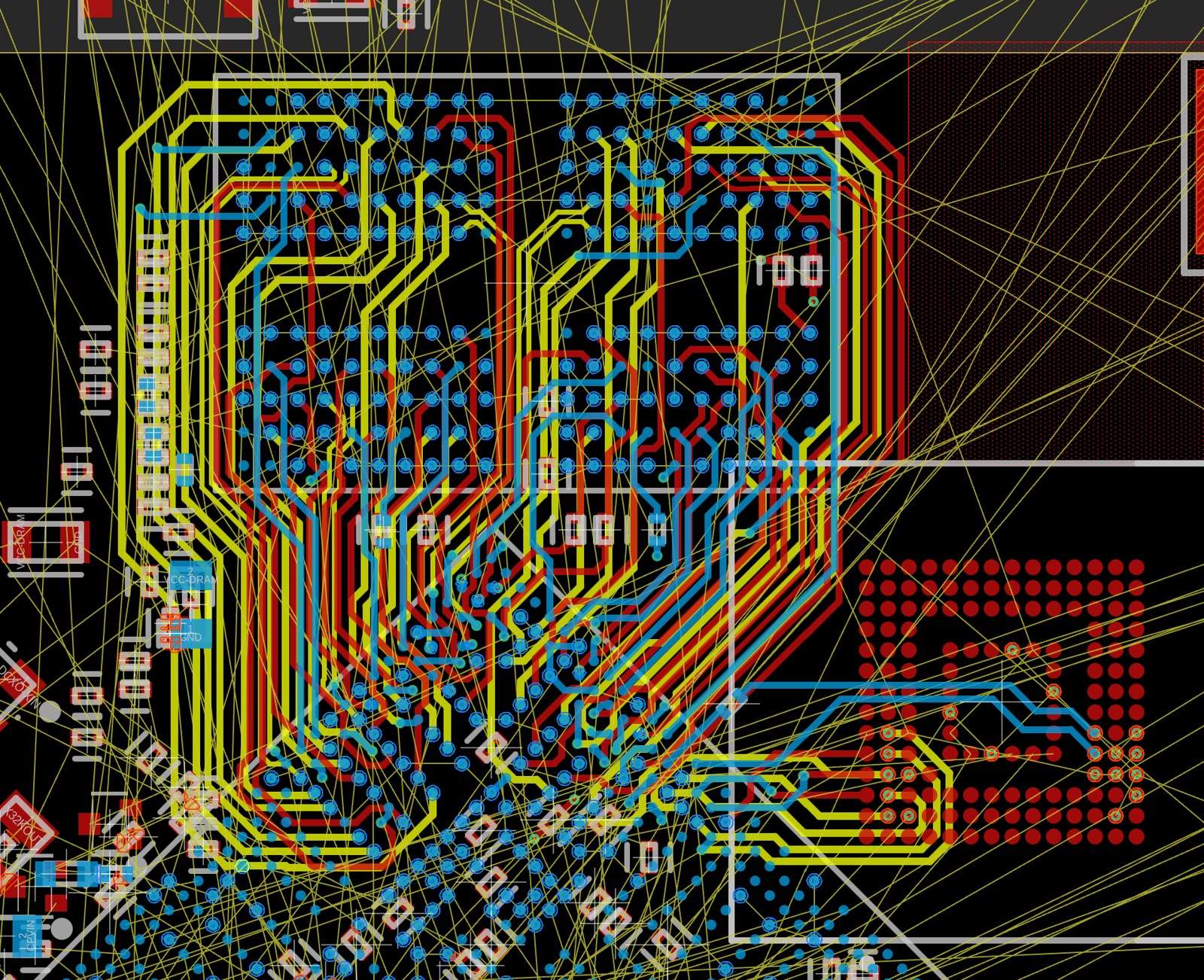
The RK3566 board has a BGA processor, two DDR3L chips, an HDMI bridge, an Ethernet switch and a Wi-Fi module on one small board, which is a lot of I/O crossing a small area. In July 2025, while we were laying out an earlier board, the conclusion was already clear: we were going to need 8 layers, especially for the data bus between the memory and the SoC. More layers meant more ground planes, and more ground planes meant cleaner impedance control.
We used JLCPCB's JLC081611-3313 stackup, 1.64 mm finished. Layers 2 and 7 are solid ground planes, and inner controlled-impedance traces only run on layers 3 and 6, each sitting next to one of those planes.
| Target | Outer layer (L1, referenced to L2) | Inner layer (L3, between L2 and L4) | Used for |
|---|---|---|---|
| 50 ohm single-ended | 0.1427 mm | 0.1605 mm | DDR3L, eMMC, RGMII, Wi-Fi SDIO |
| 90 ohm differential | 0.1468 mm wide, 0.2032 mm gap | 0.1603 mm wide, 0.2032 mm gap | USB |
| 100 ohm coplanar differential | 0.1019 mm wide, 0.1582 mm gap | 0.1087 mm wide, 0.1582 mm gap | HDMI, gigabit Ethernet, DDR3L clocks |
Those widths came from JLCPCB's impedance calculator for that stackup. The fab limits we designed to were 0.25 mm via pads with 0.15 mm holes, vias in pad, and 0.09 mm minimum trace and space.
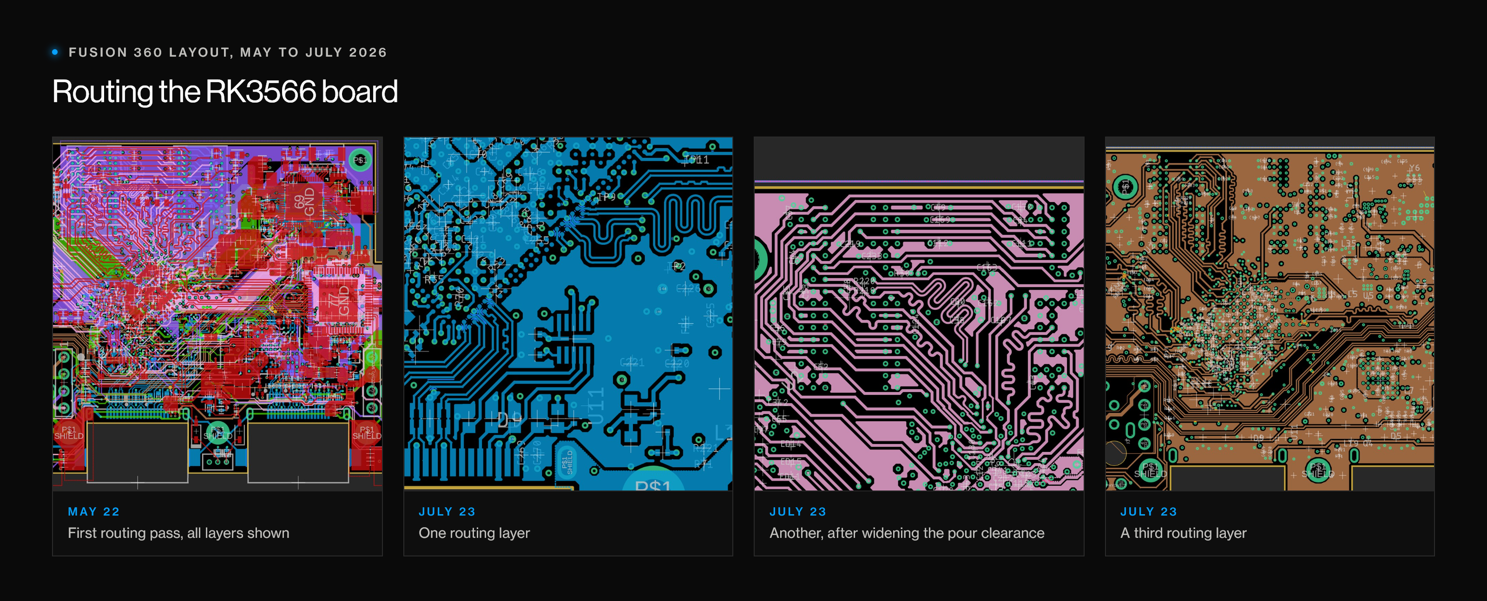
Impedance, by hand
This is where Fusion hurt. It does not do impedance calculations well, and a proper field solver is a separate paid tool. The numbers we did get out of Fusion did not agree with JLCPCB's calculator, which is the one that matters, because JLCPCB is building the board.
So most of our impedance work was manual. We set trace widths from the JLCPCB calculator, then did the length matching ourselves: read the length of every net in a group, work out the delta across all the pairs, add serpentines where a trace came up short, and check again. On a board with DDR, MIPI and HDMI, that is a lot of reading lengths off a list.
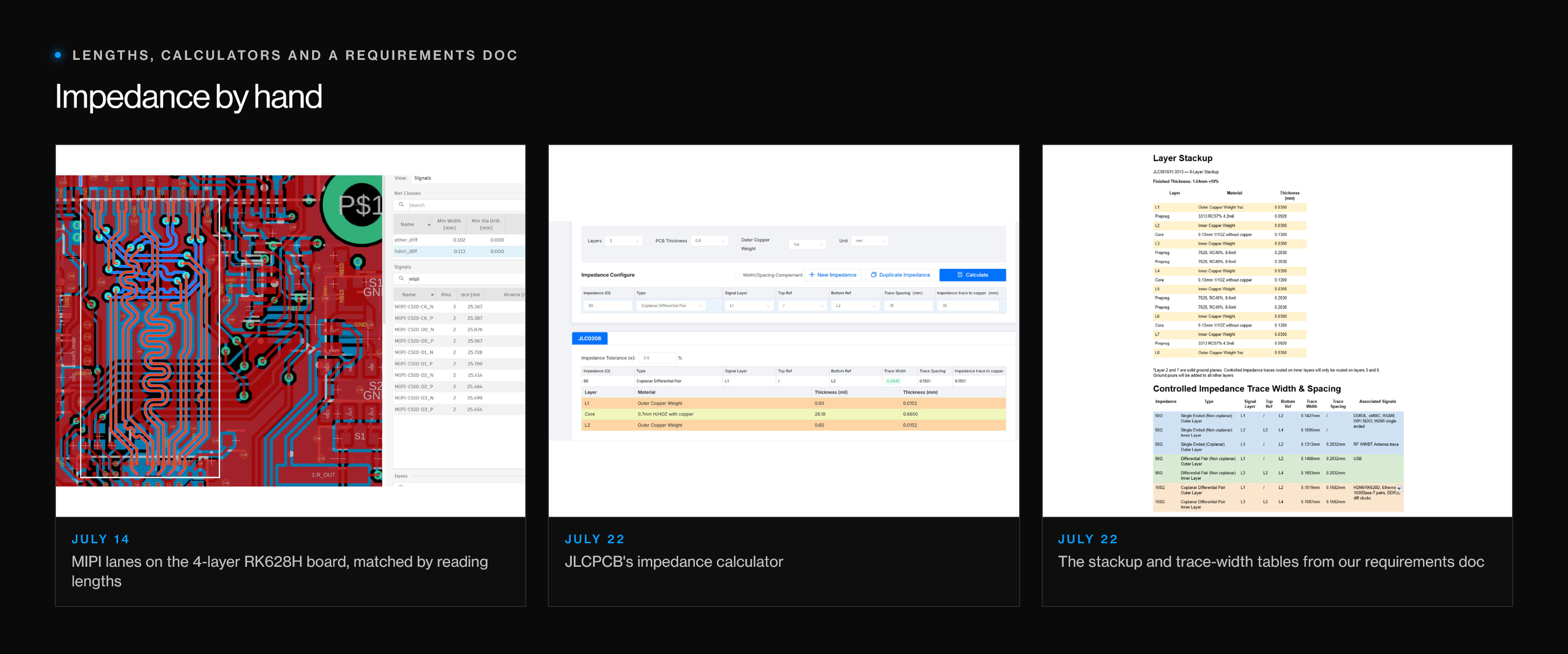
Jamie, the other half of our two-person team, put all of it into an impedance requirements document before we ordered: every controlled-impedance group, its target, its width and spacing, and its matching rules. Then Mohamed at DAT Electronics, who reviewed the board for us, imported it into Altium and verified the impedances and lengths there, a second opinion from a tool with proper impedance support. Honestly, we were about 98% of the way there. He went through a few items with Jamie, and they were mostly about margin, because we had designed right at JLCPCB's minimums. Copper clearance went from about 0.15 mm to 0.2 mm, including the ground pour next to the controlled-impedance traces. Via pads got bigger. Spacing between traces opened up to about 0.3 mm, three times the prepreg height. One DDR strobe pair needed its clearance rechecked, and the Ethernet jack's through-holes needed 3 to 5 mm to the nearest surface-mount parts for wave soldering. None of that sent us back to redo the routing, which told us the hand-matched approach in Fusion had held up.
No blind vias, until this month
Not a Fusion problem, but it shaped the layout just as much: JLCPCB did not offer blind or buried vias. With a BGA, every signal that escapes the processor on an inner layer has to go through a via that runs the full thickness of the board, and the unused part of that via is a stub that hurts signal integrity.
In September 2025 we settled on the practical answer for prototypes: route the sensitive signals on the inner layer farthest from the processor's side of the board, so the leftover via stub is as short as possible, and find a fab that could do blind vias later for production. As it happens, JLCPCB launched HDI boards with blind and buried vias this month.
What we built to cope
Two things made Fusion workable.
The first is the export. Getting a BOM and a pick-and-place file out of Fusion in the format JLCPCB wants is a pain, so we built a full library of JLCPCB parts with their part numbers attached, and scripts that generate both files straight from the design. The library of passives and those scripts are going out free in a later entry.
The second is a set of checker scripts that catch the mistakes a busy schematic hides: supply rails that only connect on one sheet, near-duplicate net names, power pins that land on unnamed nets, and crystal load capacitors that do not match the crystal. That last one has already earned its keep: on our next board, it flagged a crystal whose load capacitors did not match its spec. On the RK3566 board, the PMIC crystal's load capacitors had been set to NC in our own schematic, which is exactly the kind of thing it now catches.
// Effective load capacitance from the two caps (use first two found).
if (nCaps >= 2 && gCapVals[0] > 0 && gCapVals[1] > 0) {
real c1 = gCapVals[0];
real c2 = gCapVals[1];
real cl_eff = (c1*c2)/(c1+c2) + C_STRAY_PF;
sprintf(ln, " C1=%.1fpF C2=%.1fpF -> effective CL = %.1f pF", c1, c2, cl_eff);
PL(ln);
if (c1 != c2)
PL(" [WARN] the two load caps are not equal.");
if (target > 0) {
real dev = cl_eff - target;
if (dev < 0) dev = -dev;
if (dev > CL_TOL_PF) {
The honest assessment
Fusion's electronics workspace is EAGLE underneath, and Autodesk stopped selling and supporting standalone EAGLE on June 7, 2026. Fusion Electronics gets fairly little attention compared with the rest of Fusion. I like it because it integrates with my mechanical design, but I will admit it is behind KiCad and Altium for serious boards.
Altium is too expensive for a startup our size. A SolidWorks Electrical subscription was already a real drain on my small business last year, and I did not want another one. KiCad is free and open source, and that is a big reason to switch eventually.
For now, I am staying in Fusion to finish product development, because I am fast in it and changing tools mid-project would cost more than it saves. On the side, I am trying KiCad.
If you are choosing a PCB tool
- Pick for the loop you run most. Mine is board and enclosure together, so an integrated tool was worth a lot. If yours is signal integrity, pick the tool with the best impedance support.
- Trust your fab's calculator, not your EDA tool's. The stackup belongs to the fab, so its numbers are the ones that get built.
- Get a second set of eyes in a different tool. An independent review in a tool with a real field solver checks the numbers your own tool cannot.
- Script your exports and checks early. The time we spent on export and review scripts paid back on every order.
Next in the journal: what tariffs actually cost a hardware prototype.